
The Benefits and Challenges of Using Sensors in Semiconductor Equipment
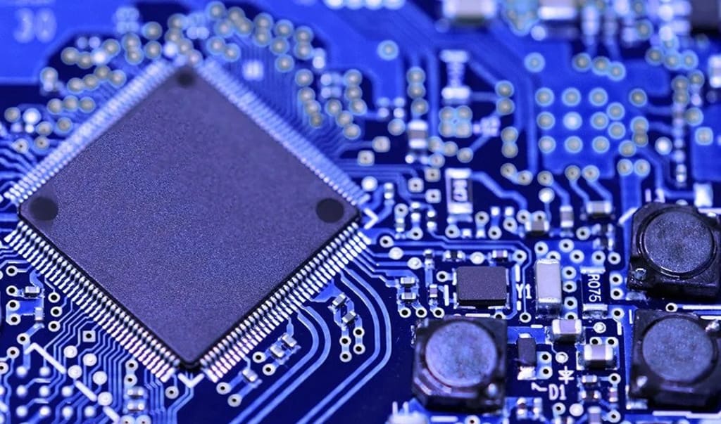
Sensors in Semiconductor Equipment

The semiconductor industry has seen explosive growth in recent years, with the demand for advanced electronics and the Internet of Things (IoT) continuing to rise. This has led to an increase in the complexity of semiconductor devices, with designs that are smaller and more intricate than ever before. As a result, semiconductor equipment makers are adding more sensors to improve fab uptime and wafer yield, reduce the cost of ownership, and minimize chip failures. By gathering data from different tools in the manufacturing process, it becomes possible to create a detailed timeline of how chips are designed, manufactured, and what goes wrong along the way.
Growth of The Semiconductor Industry and The Need for Advanced Electronics and IOT
In the semiconductor manufacturing process, a wafer goes through multiple steps to create the final product. Each step involves multiple machines and tools, each of which produces data that can be analyzed. By analyzing the data, manufacturers can identify patterns and trends that could lead to defects, and address them before they cause significant problems. This is where sensors come in. By placing sensors in the equipment, manufacturers can track the performance of each machine and tool, and collect data that can be analyzed to improve the manufacturing process.
Improving Fab Uptime and Wafer Yield with Sensors
One of the most significant advantages of using sensors in semiconductor equipment is the ability to reduce downtime. When a machine fails or requires maintenance, it can cause significant delays in the manufacturing process. By monitoring (Semiconductor Yield Monitoring) the performance of the equipment in real-time, manufacturers can identify potential issues before they become major problems, and schedule maintenance during periods of low activity. This can significantly reduce downtime and improve fab uptime.
Improving Wafer Yield and Reducing Defective Chips Produced
Another advantage of using sensors in semiconductor equipment is the ability to improve wafer yield. Wafer yield refers to the percentage of wafers that are produced without defects. Even a small increase in wafer yield can result in significant cost savings for manufacturers. By analyzing data from different tools in the manufacturing process, manufacturers can identify potential sources of defects and address them before they cause problems. This can help to improve wafer yield and reduce the number of defective chips produced.
Reducing Cost of Ownership with Sensors
The use of sensors in semiconductor equipment can also help to reduce the cost of ownership. Semiconductor manufacturing is a capital-intensive process, with equipment costs running into the millions of dollars. By monitoring the performance of the equipment in real-time, manufacturers can identify potential issues before they become major problems, and schedule maintenance during periods of low activity. This can help to extend the lifespan of the equipment and reduce the need for costly repairs or replacements.
Challenges of Implementing Sensor Networks
While the benefits of using sensors in semiconductor equipment are clear, there are challenges to implementing this technology. For example, there is the challenge of managing large amounts of data. With sensors generating data continuously, manufacturers must find ways to store, manage, and analyze this data in a way that is efficient and effective. This requires a rethinking of how and when various operations are done and why they sometimes result in defects.
Another challenge is the need to integrate different data sources. In the semiconductor manufacturing process, data is generated by multiple tools and machines. Integrating this data can be challenging, particularly when different tools use different data formats or standards. Manufacturers must find ways to integrate this data seamlessly, to get a complete picture of the manufacturing process.
Importance of Sensor Networks in Safety-Critical Markets
Despite these challenges, the use of sensors in semiconductor equipment is becoming more important, particularly as tolerances tighten at advanced nodes and in advanced packaging, and as chips are increasingly used in safety-critical markets. In these markets, quality and reliability are critical, and even small defects can have significant consequences. By using sensors to monitor the manufacturing process in real-time, manufacturers can identify potential issues before they become major problems, and ensure that the final product is of the highest quality.
Conclusion
Implementing a sensor network in a semiconductor fab can provide several benefits, including increased efficiency, improved quality, and reduced cost of ownership. However, it requires a rethinking of how and when various operations are done, and why they sometimes result in defects. Additionally, the type of sensor used and the software platform used to analyze the data are both critical to ensuring accurate and reliable data collection. As semiconductor manufacturing becomes increasingly complex, and as tolerances tighten at advanced nodes and in advanced packaging, sensor networks will become even more important for ensuring the highest levels of quality and yield.
References:
"Sensor-Based Process Monitoring: The Key to Improved Yield and Reduced Cost-of-Ownership in Semiconductor Manufacturing", KLA Corporation
"Applied SmartFactory® Rx", Applied Materials
"Enhancing Yield with Applied SmartFactory® Analytics", Applied Materials
About the Creator
Jacob Joseph
Professional Content Writer and passionate to share my knowledge with humans.
Enjoyed the story? Support the Creator.
Subscribe for free to receive all their stories in your feed. You could also pledge your support or give them a one-off tip, letting them know you appreciate their work.
Keep reading
More stories from Jacob Joseph and writers in Education and other communities.
Advanced Methods for Outlier Detection and Analysis in Semiconductor Manufacturing
The semiconductor manufacturing industry faces numerous challenges due to its complex equipment and dynamic processes. To overcome these challenges and enhance operational efficiency, there is a growing emphasis on integrating domain expertise and utilizing advanced analytical solutions. This article explores the concept of outliers in semiconductor manufacturing, delves into outlier detection methods, highlights the significance of outlier analysis in semiconductor yield monitoring, and discusses the role of semiconductor data in driving effective analytics.
By Jacob Josephabout a year ago in Education
Future Trends in Cyber Crimes, What to Watch Out For
In our increasingly interconnected world, the landscape of cyber-crimes is constantly evolving. As technology advances, so too do the tactics of cyber criminals. Understanding these trends is crucial for individuals, businesses, and governments to stay ahead in the ongoing battle against cyber threats.
By Cyber Watch7 days ago in Education
VPS Hosting 101: Everything You Need to Know
Introduction When it comes to hosting your website, the options can be overwhelming. Among the various types, VPS Hosting stands out as a popular choice for many businesses and developers. In this guide, we’ll dive deep into what VPS Hosting is, its benefits, and why it might be the right solution for your website.
By bigbirdweba day ago in Education
The Spring
The sun was high when Lance pulled off the road and into the dusty lot of the service station. The sign back at the hairpin--the first sign in a long time--said they just rolled into Hatter’s Creek, Population 63. It was small enough it didn’t appear on the handmap in Shelby’s lap, yet here it stood, the first backwater township on the fringes of the National Park. The plan was to gas up, restock the snack bag, and press on into the wilderness.
By Zack Graham6 days ago in Fiction


Comments
Jacob Joseph is not accepting comments at the moment
Want to show your support? Send them a one-off tip.