
Huawei’s New Chip Shouldn’t Be This Efficient. The Teardown Explains Why It Is.
Geekerwan sliced open the Kirin 9050 Pro. Two stacked dies, 80,000 vertical connections, and a packaging bet that could outlast the sanctions.
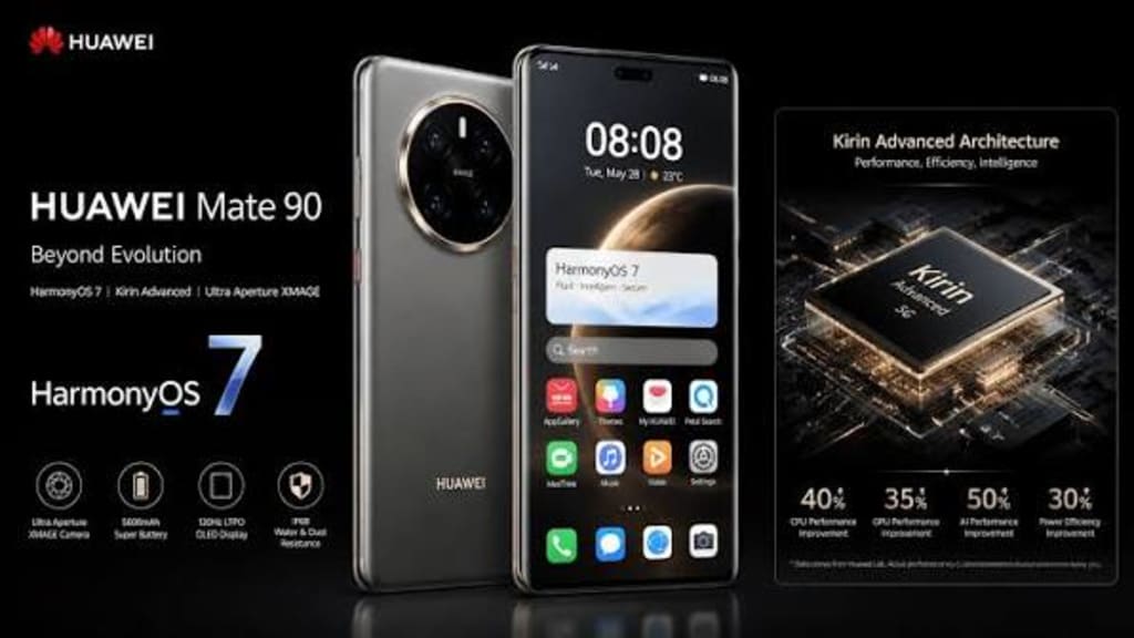
On October 2, 2026, Geekerwan published Logic Folding Deep Dive! How Strong Is Huawei’s Mate 90 Series Tao’s Law Chip? It is not a routine flagship review. The first half cuts open a Kirin 9050 Pro, images the internals with an electron microscope, and turns “logic folding” from a presentation phrase into a physical structure. The second half runs the Mate 90 Pro Max through benchmarks and games. The performance numbers matter. The teardown matters more. The teardown’s publication may matter most.
The signal in the die shot
Under the rules of the past few years, publishing die shots of a domestic flagship chip was a red line. Geekerwan’s earlier Kirin 9050 Pro review was taken down after complaints citing legal and regulatory reasons. Multiple creators had said that die-level information required clearance. This time, the video shows the two-die stack, the copper-copper hybrid bonding interface, the TSV array, and a density estimate.
Either the relevant agencies decided the sensitive window had passed, or Huawei decided the technical narrative was mature enough for public scrutiny. Either way, the video’s survival is a data point about the information space around domestic advanced chips. It suggests that the boundary around what can be discussed in public is not fixed. It has moved, at least for now.
What logic folding is
To understand the Kirin 9050 Pro, start with what logic folding is not.
Traditional 3D chip stacking, whether AMD’s 3D V-Cache or the TSMC SoIC-MH packaging expected in Apple’s M5 Pro and M5 Max, is module-level integration. A complete cache die or compute die is stacked on another die, and the layers are connected through microbumps or hybrid bonding. It is closer to stacking blocks on a PCB.
Huawei’s logic folding works at a finer grain: the unit level. According to engineering details in He Tingbo’s “Tao’s Law” V2 paper, logic folding splits the circuits of the same functional module, for example a CPU core’s arithmetic logic units and its L1/L2 cache, across different active layers. It then connects them vertically through fine-pitch hybrid bonding. In Geekerwan’s description, inside a big core, most execution units sit on the top die, while L1 and L2 cache sit on the bottom die, directly under the load/store units.
The immediate benefit is shorter signal paths. In a planar design, the route from a CPU core to cache can be measured in millimeters. After logic folding, that distance is compressed to micrometers. The paper reports a 55% reduction in global network-on-chip data path area, more than 50% fewer clock buffers, and 25% lower clock skew.
Engineering: what 1.5 micrometers means
The central process challenge in logic folding is the density of the vertical connections.
Huawei’s hybrid bonding pitch in the Kirin 9050 Pro is 1.5 μm. That number needs an industry coordinate. TSMC’s current volume SoIC bonding pitch is about 6 μm, with a plan to reach 4.5 μm by 2029. Intel’s Foveros TSV pitch is about 25 μm. Interconnect density scales inversely with the square of the pitch. Huawei’s layer-to-layer interconnect density is roughly 16 times TSMC’s current volume level.
Geekerwan’s teardown also shows another key number: about 80,000 TSVs carry power and signals between the two dies. The isolation regions for these TSVs consume about 8% of the bottom die’s usable area. The loss is measurable, but the return is larger. The two dies have the same area: 11.13 mm × 10.84 mm, about 120.65 mm² each. That single-layer area is about 37.5% smaller than the Kirin 9030 Pro, which helps single-die yield. After stacking, effective transistor density rises from 155 MTr/mm² on the Kirin 9030 Pro to 238 MTr/mm² on the Kirin 9050 Pro, a 53.5% increase. He Tingbo’s paper describes that gain as equivalent to the total from three previous years of geometric scaling.
The design choice is not accidental. Smaller dies are easier to manufacture. Two smaller dies bonded together can deliver more usable transistors than one large planar die, while keeping the thermal path manageable.
Performance: the efficiency gain is concrete, not magic
Geekerwan’s measurements support the power claims in the paper.
In measured workloads, the Kirin 9050 Pro cuts power by 66% in the NPU, 58% in the GPU, and 41% in the CPU performance core compared with the Kirin 9030 Pro. In efficiency terms, CPU single-core performance sits between the Snapdragon 8 Gen 2 and Snapdragon 8 Gen 3. CPU multi-core efficiency is almost level with the Dimensity 9400. GPU efficiency at low and medium frequencies is between the Snapdragon 8 Gen 2 and Snapdragon 8 Gen 3. In Genshin Impact, the Mate 90 Pro Max runs near full frame at an average power of 4.2 W.
The AI block also moves. Its INT8 throughput reaches 67.7 TOPS, about a 150% increase over the previous generation. Huawei claims it is the first phone SoC able to run a 30B-parameter MoE model on device.
This is not a “crush everything” result. The Kirin 9050 Pro uses SMIC N+3 for the compute die and N+2 for the cache die. Its competitors use TSMC 3 nm and 4 nm nodes. Bernstein notes that the Kirin 9050 Pro beats Apple’s A17 Pro from 2023, which used a 3 nm process, in Geekbench 6 multi-core. It still trails the latest 2 nm A20 Pro by roughly 30%.
The gap has been kept within an acceptable range, and in efficiency the direction has reversed. The gain comes from architecture, not process.
Huawei vs. TSMC: different roads
Jensen Huang was asked about “Tao’s Law.” His answer: “For Huawei it’s a breakthrough, but for TSMC it’s not a threat.” That is partly true, but it needs a finer reading.
TSMC is not ignoring 3D stacking. Its SoIC technology has been in volume since 2023, and its interconnect density is more than 56 times higher than 2.5D packaging. Apple’s M5 Pro and M5 Max are expected to be among the first SoCs to use SoIC-MH, separating CPU and GPU modules. Qualcomm’s Snapdragon 8 Elite Gen 6 is adopting Offset PoP packaging to create more thermal room.
But TSMC’s 3D stacking remains packaging-level. It integrates already-finished chips or modules vertically. Huawei’s logic folding breaks the planar layout at the design stage. It distributes the circuits of one logic function across layers.
That difference decides how the two roads evolve. TSMC’s SoIC benefits from the most advanced nodes. Every process shrink lifts SoIC performance and efficiency. Huawei’s logic folding extracts extra performance from existing nodes. Its ceiling is limited by the underlying transistor performance.
The reverse is also true. Logic folding gains stack on top of process progress. If Huawei later gains access to a better process, through domestic equipment breakthroughs or another path, the folding gains amplify on that base. He Tingbo’s paper predicts that by 2031, high-end chips based on Tao’s Law will reach transistor density equivalent to a 1.4 nm process.
Costs and limits
He Tingbo’s paper admits that “describing τ scaling as a completed system would be misleading.” Several substantial problems remain open, including toolchains and methodology, wafer-to-wafer process variation, and vertical interconnect overhead.
The most urgent problem is cost and yield.
Logic folding requires two dies to be manufactured separately, then bonded at wafer level. If a single die yields at 50%, the combined theoretical yield after bonding can fall to about 25%. That is why the Kirin 9050 Pro appears only in the Mate 90 Pro Max and RS Ultimate Design. Huawei cannot yet spread the cost across the entire lineup.
Thermal management is another ongoing challenge. The paper mentions “thermal-aware partitioning and floorplanning.” High-power circuits are deliberately kept from becoming spatially adjacent. Geekerwan’s teardown confirms the approach: compute units are on the top die, where cooling is easier; cache and I/O are on the bottom die, where heat generation is lower.
A more fundamental limit is that logic folding addresses signal delay. It does not directly raise transistor switching speed. In Geekerwan’s comment section, one viewer put it accurately: 3D folding can increase transistor count, but it cannot reduce the speed of information communication. More precisely, logic folding reduces the delay and power of layer-to-layer signal transmission, not the performance of the transistor itself. That means the largest gains appear in massively parallel and cache-heavy workloads. Single-thread peak performance gains are more limited.
The Kirin 9050 Pro’s big core runs at 3.1 GHz. Qualcomm’s flagship at the same time is above 5 GHz. Huawei may not be unable to push frequency higher. It may be choosing a more conservative frequency strategy because logic folding gives it efficiency to trade for battery life, and architecture to trade for process.
Strategic meaning: a third road forced by sanctions
Five years ago, few would have predicted that Huawei would return to the flagship chip table through “logic folding.”
U.S. export controls cut Huawei off from EUV lithography and TSMC’s advanced nodes. Under the traditional semiconductor roadmap, Huawei’s chip performance should have been locked near 7 nm, with the gap to Apple, Qualcomm, and MediaTek widening every year.
Sanctions produced an unintended result. They forced Huawei to rethink chip design from every link in the chain. EDA tools, IP cores, and process libraries all default to planar design. For Huawei, all of them had to be rebuilt. Rebuilding from scratch created the chance to integrate vertically across the whole stack.
TSMC does not do logic folding today. That is not because it is technically impossible. The larger reason is ecosystem inertia. Every tool, design flow, and piece of intellectual property assumes planar chips. TSMC has no need to switch, because its customers still get performance gains from each process generation on planar designs.
Huawei does not have that option. When geometric scaling is blocked, time scaling becomes the only direction.
There is a parallel with HarmonyOS. Sanctions accelerated Huawei’s move away from Android, and the distributed architecture of HarmonyOS ended up creating a differentiated experience. Logic folding follows the same logic. A path chosen under pressure may turn out to be a forward-looking direction for the next generation of chip design.
An open invitation
Geekerwan’s video has its highest technical value in the teardown. Its most informative element may be that it could be published at all.
Die shots moving from “red line” to “discussable” can mean several things. It may mean Huawei is confident enough in its technical path that it no longer fears dissection. It may mean the relevant agencies decided that after Tao’s Law was established through academic papers and launches, letting the public see physical evidence would strengthen credibility rather than weaken control.
Whatever the reason, for people watching China’s semiconductor industry, the video’s survival is a measurable shift. The Kirin 9050 Pro is not a perfect chip. Its single-core performance still trails. Its cost is still high. Its yield is still fragile. But it is the first mass-market phone chip to use architectural innovation to reverse efficiency while at a process disadvantage. Its existence is a concrete answer to the question “after Moore’s Law, what next?”
He Tingbo closes the paper with this: “Many open questions remain, and no single organization can solve them alone—toolchains, standards, benchmarks, device physics, and economic models all require contributions from beyond any one company. This paper is therefore both a report from the front line of practice and an invitation.”
Whether that invitation is accepted will decide whether logic folding remains a Huawei-only case or becomes the next standard for the industry.
About the Creator
Jin
Writer of reamstories
https://reamstories.com/jin
Enjoyed the story? Support the Creator.
Subscribe for free to receive all their stories in your feed. You could also become a paid subscriber, letting them know you appreciate their work.
Comments
There are no comments for this story
Be the first to respond and start the conversation.