
Your camera has a 1945 bottleneck. Ferroelectric pixels could cut it.
Machine vision can do its first math inside the sensor array. The hard part is making that array reliable enough for a chip that runs for years.
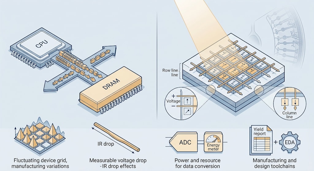
The memory wall shows up as a set of costs you can calculate
The von Neumann architecture stores instructions and data together in memory. The CPU fetches instructions, fetches data, performs operations, and writes results back. This design gives computers generality. The price is that every operation requires data to move between the processor and memory.
Early workloads could ignore that price. A 1920×1080 image changes the accounting. In a 3×3 convolution, each output pixel needs nine input pixels and nine weights. The weights are reused across the image. Data movement exceeds the actual computation, and the processor spends most of its time waiting for data.
The energy cost makes the problem concrete. In advanced process nodes, a 32-bit floating-point multiply-accumulate costs picojoules. An off-chip DRAM access can cost hundreds of times more. A commonly cited order-of-magnitude illustration puts a 32-bit multiplication at about 3.1 pJ, a 32-bit SRAM read at about 5 pJ, and a 32-bit DRAM read at about 640 pJ. These are illustrations, not precise measurements. They still show where the energy goes in data-intensive work: moving data, not computing on it.
Bandwidth adds a second constraint. Processor performance has grown with Moore’s law. DRAM bandwidth has lagged. The gap is the memory wall. Compute idles when data cannot reach it.
Vision tasks hit both constraints. A high-definition frame contains millions of pixels. A video stream keeps producing them. Convolution and pooling are repetitive and parallel in principle, but data supply limits them. Autonomous driving needs millisecond perception. Industrial inspection runs on tighter cycles. Data cannot queue on the bus.
The question becomes practical: can computation happen where the data sits? Compute-in-memory starts there.
Compute-in-memory hands multiply-accumulate to physical laws
Compute-in-memory embeds computing capability inside memory, or storage capability inside the compute array. The goal is to reduce data movement between processor and memory.
The crossbar array is the common analog structure. A read voltage is applied to row lines. Current is collected on column lines. The conductance at each intersection represents a weight. Ohm’s law gives the output current as input voltage times conductance. Kirchhoff’s current law sums the currents on each column. The weighted sum, the core operation in neural networks, happens in parallel in the physical array.
Physical parallelism still has a cost. The cost moves from data movement to device non-ideality, IR drop, leakage current, analog-to-digital conversion, and calibration. The engineering problem is whether those shifted costs stay controllable.
That boundary defines the fit. Compute-in-memory suits tasks with fixed or infrequently updated weights, matrix-vector multiplication, and tolerance for reduced precision. Tasks that need high-precision floating point, frequent weight updates, or complex control flow still need digital processors. A practical system will be heterogeneous: the compute array handles matrix operations, and digital units handle control, nonlinearity, precision correction, and protocols.
In-sensor computing pulls sensing into the same physical carrier
Compute-in-memory addresses the split between computing and storage. Vision has a third link: sensing. The conventional chain runs from photoelectric sensor to digital signal to processor to storage to computation. Every transfer consumes bandwidth and power.
In-sensor computing gives the sensor device sensing, storage, and computation. Preliminary processing happens where the optical signal becomes an electrical signal. The first convolution or fully connected operation can finish inside the array before the image is fully read out.
Ferroelectric materials fit this role for three physical reasons.
Ferroelectric polarization has multiple stable states and holds them without power. Compared with volatile SRAM, it does not need continuous power to keep weights. Compared with floating-gate devices, ferroelectric switching has lower energy potential.
The photoelectric response can be tuned by polarization. Photogenerated carrier transport in a ferroelectric thin film depends on the polarization state. The stored weight can affect the sensed signal. This coupling separates in-sensor computing from a sensor plus a separate compute array.
HfO₂-based ferroelectrics are compatible with standard CMOS. That compatibility supports large array integration. Polymer ferroelectrics such as P(VDF-TrFE) have potential in flexible substrates and wearable devices. The material choice decides whether the device targets high-density logic compatibility or flexible, biocompatible use.
At the array level, each pixel becomes a programmable compute node. Light enters the ferroelectric optoelectronic layer and generates photocurrent. The polarization state stores a weight. The output current approximates light intensity times weight in the analog domain. The array is organized as a crossbar, and currents on each column sum automatically.
The conventional comparison is straightforward. A CMOS image sensor with a digital processor sends each full frame to the processor. It stores weights in off-chip DRAM or on-chip SRAM. It performs multiply-accumulate through sequential digital operations. Power is high and dominated by data movement. Precision is high and digitally deterministic. The technology is mature and suits general vision and high-precision tasks.
A ferroelectric optoelectronic in-sensor compute array performs preliminary operations inside the array. It stores weights as non-volatile polarization states. It performs multiply-accumulate through analog physical parallelism. Power has potential to drop, but peripheral circuits constrain the result. Precision suffers from device non-ideality. The technology sits between laboratory validation and small-array demonstration. It suits edge screening and low-power always-on sensing.
The comparison points to a narrow fit. In-sensor computing works best for first-layer feature extraction, event screening, and always-on sensing. Those tasks tolerate some precision loss and care about energy and latency. The array does not replace high-precision back-end processing.
The retina offers an architecture, not a metaphor
The human retina is not a camera. After hundreds of millions of photoreceptors, several neuron layers process the signal locally: bipolar cells, horizontal cells, amacrine cells, and ganglion cells. Edge enhancement, contrast adaptation, and motion detection happen before the signal reaches the brain.
The retina is a highly parallel analog computing chip. It consumes about 20 milliwatts and processes a large visual stream in real time. Neuromorphic vision borrows its organizing principle: sensing is computing, and computing is storage.
A ferroelectric optoelectronic array runs a five-step workflow. Electrical pulses write weights by modulating polarization. Light illuminates the array and generates photocurrent related to intensity and polarization. Kirchhoff’s current law sums the column currents in the analog domain. Comparators, ADCs, or spike circuits convert the result into digital features or events. Digital accelerators, compute arrays, or spiking neural networks handle the back end.
The image is never fully read out and sent in. The first layer of computation finishes inside the array.
Spiking neural networks form a second branch. Dynamic vision sensors output events only when pixel brightness changes, so the output is sparse. Ferroelectric multi-state devices can mimic synaptic plasticity. Together they can build a sensing, computing, and storage system where the event stream drives weight updates and membrane potential accumulation without clock-synchronized full-frame processing. SNN training algorithms, event encoding, and hardware mapping tools remain immature. The combination of in-sensor arrays and SNNs is still mostly proof-of-principle and local module validation, not a general neuromorphic vision chip.
A useful analogy: a conventional vision system takes a photo, develops it, then sends it for analysis. Neuromorphic vision completes a preliminary judgment at the moment of seeing. The analogy has a boundary. The eye’s first judgment cannot replace the brain’s deep reasoning. In-sensor computing handles front-end screening and feature extraction, not all of visual intelligence.
Edge AI cares about energy efficiency before absolute compute
Edge AI devices face hard constraints. Power runs from milliwatts to watts. Compute is limited. Devices often run on batteries or harvested energy. Applications keep getting heavier: face recognition in smart locks, health monitoring in wearables, obstacle avoidance in drones.
Energy efficiency, measured in TOPS/W, matters more than absolute compute. Compute-in-memory gains efficiency through two subtractions. Weights stay inside the compute array, so they do not move from memory for every operation. Analog multiply-accumulate produces intermediate results that stay in place until analog-to-digital conversion is needed.
Under ideal conditions, those subtractions can improve energy efficiency by one to two orders of magnitude. ADC and DAC overhead, array scale, precision requirements, and calibration strategy decide the real result. Peripheral circuits often set the chip’s power budget, not the array.
Several scenarios show where the fit matters.
Smart security and access control can run face detection continuously on a low-power in-sensor array. The back-end recognizer wakes only when a face appears. The system saves always-on power and upload bandwidth, and it reduces privacy exposure.
Industrial visual inspection can screen defects at the sensor end. High-speed line cameras produce large image volumes. Front-end screening reduces back-end compute demand. On a high-speed line, latency matters more than throughput, and screening shortens response time.
Autonomous driving can preprocess and screen targets near the camera. Multi-camera data then reaches the in-vehicle platform with less bandwidth pressure. In-sensor arrays fit low-level feature extraction and motion-event detection. The back end receives sparser input with more information per bit.
Wearables and implantable medical devices need long-term monitoring at low power. Retinal prostheses and smart contact lenses are examples. Flexible ferroelectrics and biocompatible packaging decide whether those devices become practical.
Four engineering barriers, each with concrete failure modes
Device variation comes first. Ferroelectric domain switching differs across pixels. The same weight behaves differently on different cells. Larger arrays make the variation harder to ignore.
Cycle-to-cycle variation follows. Writing the same weight to the same device multiple times produces random conductance fluctuations. Weights that update often suffer directly.
Retention and fatigue set reliability limits. Ferroelectric polarization can depolarize over time. Repeated switching causes fatigue. Automotive and medical applications treat long-term reliability as a hard gate.
Linearity and symmetry affect training and inference. Ideal weight updates are linear and symmetric. Real device conductance updates are often nonlinear and asymmetric. Training convergence and inference precision pay for that mismatch.
Array and circuit effects add more error. Parasitic resistance on row and column lines causes IR drop. Distant cells receive voltages that differ from the design value. Larger arrays make IR drop worse.
Leakage current and crosstalk contaminate the column sum. Unselected cells are not perfectly isolated. Selector devices or compensation algorithms reduce the error. Selectors add process complexity and area.
ADC and DAC overhead can erase the analog advantage. High-precision conversion costs power and area. Many compute-in-memory chips spend most of their power in peripheral conversion circuits, not the array.
Dark current and illumination non-uniformity add an optical layer of error. Photoelectric sensing introduces dark current and response variation. Those errors sit on top of an already fragile analog signal. In-sensor computing carries one more non-ideality than purely electrical compute-in-memory.
Algorithm and system design must compensate. Hardware-aware training models device noise and nonlinearity in the forward pass. The network learns to tolerate hardware defects. Error compensation and calibration correct systematic deviation through on-chip circuits or software. Calibration frequency and cost must match the precision target. Hardware-software co-design tunes quantization bit width, sparsity, and array mapping to the hardware. A digital network mapped directly onto an analog array often performs poorly.
Ecosystem barriers decide whether the technology reaches products. Process yield and consistency must hold from a single laboratory device to a million-cell array. Material, process, and packaging variation amplify at array scale.
Design tools lag. Traditional EDA tools do not yet support analog compute arrays well. Standardized modeling and simulation flows are missing. Designers build device and array models themselves, which is slow and hard to reuse.
Evaluation standards differ. Teams report energy efficiency and precision with different definitions. Array efficiency differs from system efficiency. Inference precision differs from training precision. Comparisons need clear boundaries.
Application validation takes years. Automotive and medical certification require reliability, lifetime, temperature range, and electromagnetic compatibility testing. Prototypes do not become products until those tests pass.
The barriers form a chain: device non-ideality, array parasitics and peripheral overhead, algorithm co-design and calibration, process yield and toolchain, then application certification and ecosystem. A failure at any layer keeps the technology in the lab.
The path is layered, and the timeline lives in yield reports
The sequence is direct. The memory wall comes from data movement caused by separated computing and storage. Compute-in-memory moves computation to the data. In-sensor computing moves sensing into the same physical carrier, so an image can complete a preliminary weighted sum as it forms. A ferroelectric optoelectronic array stores weights in polarization, carries input through photoelectric response, and sums currents through Kirchhoff’s law.
A laboratory device and a chip that runs for years in an edge device are different objects. Device non-ideality, array parasitics, algorithm co-design, process yield, and toolchain ecosystem separate them. Materials scientists, device engineers, circuit designers, and algorithm researchers have to work together.
The industrial path will likely be layered. Validate always-on sensing, front-end screening, and low-power event detection first. Then move to higher precision, larger arrays, and more complex tasks. Digital processors will remain. Compute arrays will not cover every workload. Heterogeneous systems and hardware-software co-design are the practical form.
Neuromorphic vision aims for a machine eye that runs at low power, low latency, and thinks while seeing. Compute-in-memory and in-sensor computing are one route. The route matters because it grounds biomimicry in device physics rather than analogy.
Mass production within five years will depend on yield reports and EDA toolchain updates. Conference papers will not decide it.
About the Creator
Jin
Writer of reamstories
https://reamstories.com/jin
Enjoyed the story? Support the Creator.
Subscribe for free to receive all their stories in your feed. You could also become a paid subscriber, letting them know you appreciate their work.
Comments
There are no comments for this story
Be the first to respond and start the conversation.