
Jensen Huang Says China Will Build Advanced Lithography by 2030. Zeiss Says 15 Years. Here’s What’s Actually Happening.
DUV tools are already shipping. EUV is still in the lab. The fight is over the 70% of chips the world still needs.
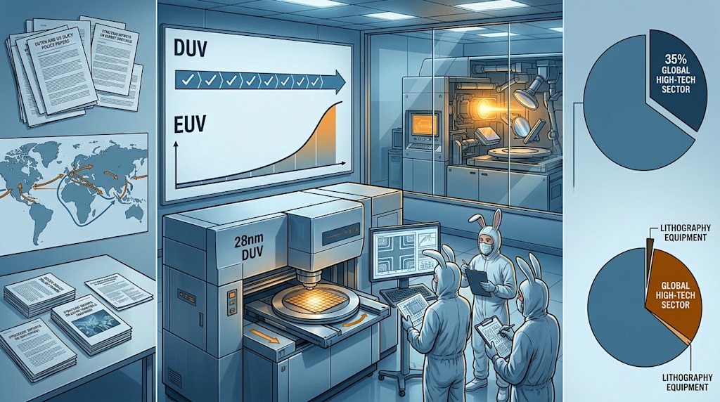
A misunderstood judgment
In September 2026, Nvidia CEO Jensen Huang was asked at the All-In Summit when China would finish advanced lithography tools. He said 2030. He added that once the technology matures, China can manufacture at scale, and domestic tools will enter local fabs.
Around the same time, Frank Rohmund of Zeiss Semiconductor gave a different number: 15 years. Zeiss supplies the mirror assembly for ASML’s EUV machines and holds a near monopoly on EUV mirrors. Rohmund’s estimate uses ASML’s own timeline as a benchmark. ASML started EUV research in 1997 and delivered its first mass production tool in 2016, nearly two decades later. Rebuilding an embargoed supply chain from zero makes 15 years a reasonable estimate.
The two numbers look like a generational disagreement. They describe different scopes. Huang said “advanced lithography systems.” SEMI standards use that phrase for both immersion DUV and EUV. Rohmund answered about EUV specifically. The question is how far China’s lithography has actually moved between those two anchors.
DUV: delivered, not promised
May 2026 is the month China’s lithography effort delivered. Shanghai Micro Electronics Equipment completed the first batch delivery of its SSA800 series 28nm immersion DUV tool and moved into mass production validation. The tool passed a full technical acceptance by a Ministry of Industry and Information Technology panel in July 2025. SMEE announced full production in January 2026 at the Yangtze River Delta Semiconductor Industry Summit. Yield is above 90%. The tool appeared publicly for the first time at SEMICON China 2026.
The specs matter. The SSA800 uses 193nm ArF immersion. It supports 28nm in one exposure and extends to 14nm with multiple patterning. Overlay is 2.3 to 2.5nm. Throughput is 150 wafers per hour. Local content is above 85%, and the three core subsystems are domestically developed and built. The 2026 plan calls for five units. Capacity expands to more than 20 units in 2027. First customers include SMIC, Hua Hong Semiconductor, and ChangXin Memory Technologies. They will use the tools for power semiconductors, memory, and automotive MCUs.
The context gives those numbers weight. Chips at 28nm and above are about 70% of global chip demand. China already holds close to 30% of capacity in that range. The SSA800 covers the highest volume part of the market. China had depended on ASML immersion DUV tools there. The MATCH Act aims to control all immersion DUV models sold to China. The SSA800’s delivery hedges that cutoff risk.
The supply chain effect may matter more. A high end lithography tool sells for about $150 million. Photoresist, optics, and wafer stages are nearly 60% of that value. SSA800 volume releases orders for light sources, lenses, dual wafer stages, motion control, immersion systems, and tens of thousands of parts. The tool starts a chain.
EUV: subsystems closed, whole machine still climbing
EUV is the harder problem. It uses more than 100,000 parts. It needs reflective imaging in vacuum, stable plasma light, and magnetic levitation wafer stages with nanometer positioning.
Public progress points to one conclusion: core subsystems have closed the technical loop. The whole machine is moving from prototype to engineering verification.
The light source is the heart. Lin Nan’s team at the Shanghai Institute of Optics and Fine Mechanics uses a solid state laser driven LPP route. They reached 3.42% conversion efficiency at 13.5nm. That is about 60% of ASML’s commercial CO2 driven source. The route matters. Solid state lasers differ from ASML’s CO2 approach in size, efficiency, and patent landscape. It may avoid some patent barriers. On the industrial side, RSLaser’s 250W class EUV plasma source completed a 1,000 hour stability test. Its conversion efficiency and particle control are reported to meet ASML NXE:3600D entry level. The lab number, 3.42%, is far from the 250W stable output needed for production. The direction is clear.
Optics have also moved. The Changchun Institute of Optics, Fine Mechanics and Physics and MLOptic developed an EUV multilayer reflective objective with 0.1nm surface figure accuracy and 99.9% reflectivity. Before this, only Zeiss made EUV grade mirrors. The objective numerical aperture is 0.75. Making one qualified mirror is not the same as mass producing and integrating it into a stable machine. That engineering road remains.
On wafer stages, U-Precision’s sixth generation magnetic levitation dual stage reaches 0.1nm positioning and 70 wafers per hour. It has run on 28nm immersion tools for more than two years. EUV grade motion control has already been validated on DUV platforms. DUV production is the training ground for EUV.
At the whole machine level, SMEE’s first EUV prototype produced light in the second half of 2025. It completed a full 13.5nm exposure flow. The team is working on three items: raise continuous source power from 200W to 300W, improve overlay through multi mirror alignment to push throughput above 100 wafers per hour, and adapt the machine to cleanroom conditions. At that pace, the first engineering verification machine for fab tape out could arrive in the second half of 2027.
Engineering verification is not production maturity. UBS analysts judge from patent activity that China’s EUV maturity is near ASML’s 2004 stage. Stable commercial use is more than ten years away. RAND puts the probability of Chinese EUV production by 2030 at 10%. It found 45% of respondents expect that after 2030. Those estimates line up with Zeiss’s 15 years.
The base: 35% installed, 1% lithography
Lithography cannot be separated from the rest of the equipment base. In 2026, domestic tools rose to 35% of installed equipment in Chinese fabs. The number measures the installed base, not one tender. Three years ago it was about 10%.
The average hides a split. Stripping tools are above 80% local. Etch and cleaning are 50% to 60%. Lithography is below 1%. Metrology and inspection are below 10%. The strongest and weakest segments differ by about 80 percentage points. On new 12 inch lines, domestic tools are about 55% of tenders. Etch is 65%, deposition 61%, cleaning 63%. The gaps show the easy to hard path of localization.
The mature and advanced split matters more. For 28nm and above, domestic equipment is past half. For 14nm and below, etch self sufficiency is below 15%. Lithography, especially EUV, is the hardest ceiling. Etch, cleaning, and deposition can substitute on DUV platforms and form a commercial loop. Every lithography step upward requires reopening the chain from light source to optics to wafer stage.
The base is still thickening. In the first half of 2026, eight major equipment companies grew revenue by 13.8% to 69%. Leading firms have order backlogs into 2027. Mainland China has been the largest semiconductor equipment market for six straight years since 2020. Sales in 2025 were about $49.3 billion, or 36.5% of the world. Scale funds iteration.
The external fight: MATCH and the Netherlands
Export controls frame all of this. The MATCH Act in the U.S. House would expand controls from EUV to all ASML immersion DUV models. It would also ban Western firms from providing software upgrades, spare parts, and maintenance for installed tools in China. That hits ASML’s service business. Maintenance and upgrades are the long term profit pool.
Dutch Prime Minister Rob Jetten opposes the bill. He told Bloomberg TV in New York that he has discussed MATCH with Trump and U.S. lawmakers. He said, “I am very confident that we can eventually reach an agreement that works for all parties.” His logic: the Netherlands already imposes strict controls on ASML. It must also protect its semiconductor industry. In the second quarter of 2026, China was 14% of ASML’s net system sales, down from 19% in the first quarter. Tighter controls push that share toward domestic tools.
A Washington think tank adds pressure from the other side. The Center for Technology and National Security Governance says Chinese fabs had 343 DUV tools by early 2026. If imports continue, by 2035 those tools could support capacity equal to 434 million Nvidia H100 AI chips per year. The report recommends stopping DUVi exports to China because current controls have loopholes.
The tightening has sped up a decision inside Chinese fabs. Domestic tools moved from alternative to default. MIIT documents say that from late 2025, new wafer capacity must source at least 50% of equipment domestically. Tender based localization jumped. Policy and tool maturity reinforce each other.
Two timelines, one supply chain
The four layers give a clearer picture than “2030 versus 15 years.”
DUV has delivered. The SSA800 moves domestic immersion lithography from usable to mass producible. The 2027 plan for more than 20 units points to area wide substitution in mature processes. This timeline no longer needs forecasts.
EUV is still climbing. Subsystems have closed the loop. That is not maturity. A 3.42% source and a single 0.1nm mirror must become a 250W stable source and a whole machine with overlay control. Zeiss’s 15 years and RAND’s 10% chance by 2030 describe the same steep curve. A realistic view: EUV moves from engineering verification to stable production in the early to mid 2030s. Huang’s 2030 claim works if it means full DUV substitution plus a working EUV prototype.
The long term effect comes from the link between the two timelines. DUV production gives EUV cash, line data, and a tested engineering team. U-Precision’s wafer stage ran on 28nm lines for two years before adapting to EUV. RSLaser moved from DUV excimer lasers to EUV plasma sources. SMEE’s integration experience runs from SSA800 to EUV engineering machines. ASML did not have that path. It started from zero. China starts from a 28nm base.
Huang said it is a matter of time. That is correct. The open question is how much of the global equipment market changes while that time passes.
About the Creator
Jin
Writer of reamstories
https://reamstories.com/jin
Enjoyed the story? Support the Creator.
Subscribe for free to receive all their stories in your feed. You could also become a paid subscriber, letting them know you appreciate their work.
Comments
There are no comments for this story
Be the first to respond and start the conversation.