
Inside Tesla’s Insane $119 Billion Gamble to Build the World’s Largest Chip Factory
The white line rising from the Texas dust isn't just a factory. It's a do-or-die bet against TSMC, ASML, and the laws of physics—with 75% of its chips headed straight for outer space.
Opening: A Factory That Doesn't Look Like a Factory
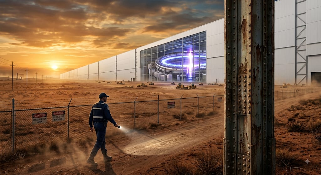
If you look out from the county road in Grimes County, Texas, the first thing you see won't strike you as a chip factory.
It's too long. Like a white straight line someone drew with a ruler across the reddish‑brown earth. The factory building hugs the ground and stretches out, all the way to the horizon, with no sign of turning. Long rectangular structures flank both sides in symmetrical formation, leaving a wide gap in the middle. From a distance, it looks more like an airport terminal being expanded, that endless corridor on one side of Pudong Airport.
Along the outer edge of the site, construction fencing still stands. Bulldozers cast short shadows under the midday sun, and the air carries a mix of dust and the residual heat of burning diesel. No one lingers too long by the site in that heat. But if you stop, you notice one detail: the factory walls are much thicker than ordinary industrial buildings. Not thick for load‑bearing reasons; thick because they were designed to run a straight vacuum pipe through the interior.
This is Terafab. On August 6, 2026, SpaceX's official website confirmed its existence with a press release of fewer than two thousand words: Grimes County, Texas, groundbreaking officially underway.
The numbers in the release lined up coldly: initial investment of $16.8 billion, with a long‑term potential of $119 billion, planned manufacturing floor space exceeding 100 million square feet. What the release didn't mention was that three months earlier, in April 2026, Tesla had already quietly broken ground on a pilot R&D wafer fab called ATCF just north of its Texas Gigafactory, a much smaller testbed. By the time the August announcement came out, the first underground pipelines had already been laid at ATCF. In less than five months, Musk had turned a ring‑shaped structure from a concept render into a real foundation rising from the soil of Grimes County.
That afternoon, when the news broke, everything at TSMC's Fab 18 in Tainan continued as usual. The gowning‑in and ‑out procedures didn't change. The temperature controls inside the lithography machines didn't change. The frequency at which tin droplets were hit by lasers didn't change. But outside the fab gates, semiconductor industry analysts started flipping through an old file again.
II. Fifty Times
One phrase in the announcement unsettled people: "1 terawatt of compute."
That's not a unit the chip industry is used to. Wafer fabs talk about monthly capacity in thousands of wafers, yield in percentage points, process nodes in nanometers. Musk talks about compute. He directly converts chips into the total amount of processing power they can deliver.
What does 1 terawatt mean? Analysis firms ran quick calculations that same afternoon: roughly 50 times the current annual global chip production. In other words, even if this factory ran at only half its target capacity, it would be like having 25 extra Earths making chips out of thin air. That analogy made a lot of people pause with their fingers over their keyboards, and then keep typing.
Musk had floated an even more absurd number earlier: 1 petawatt, or 1,000 terawatts. That was his word for the "long‑term vision," roughly equivalent to 300 times humanity's current total electricity consumption. Numbers like that read like sci‑fi world‑building in tech news, but look ridiculous next to real‑estate transaction records. So the announcement only wrote 1 TW, still absurd, but not so absurd that it made the release feel like promotional material for the next Dune movie.
The capacity allocation was spelled out like this: 25% for Earth, 75% for space.
The Earth‑side half includes Tesla's Optimus humanoid robots and Cybercab self‑driving taxis. Optimus needs little explanation; its prototype is already standing by the assembly line at the Fremont factory in California, able to pick up parts from the conveyor belt, watch humans perform tasks, and then learn to do them. The Cybercab has no steering wheel, a detail that was repeated at Tesla's product launches.
The space half requires a bit more imagination. SpaceX plans to build a distributed AI supercomputer using one million low‑orbit satellites. Every satellite will carry chips that can't be afraid of space radiation, can't be afraid of wild temperature swings from sub‑zero to positive, and have to withstand far more in vacuum than anything on the ground. Terafab will produce a dedicated space‑grade chip codenamed "D3" to meet those requirements.
The process node was also set: Intel 14A. 1.4 nanometers, full High‑NA EUV integration, slated for volume production in 2028. For Intel, this is a critical window; they're transitioning from IDM to foundry services, and Terafab is the largest order they've landed. But for TSMC, it means a major client who used to buy chips from them is now building their own furnaces.
A reporter asked TSMC Chairman C.C. Wei on an earnings call how he viewed Terafab. He said only two words: "No shortcuts."
Musk fired back on social media that same day: Terafab will always be TSMC's largest customer, not a competitor.
The words came fast, fast like a wave of the hand. Not many people really believed it.
III. Changing the Light
What really made semiconductor engineers put down their coffee cups wasn't the capacity; it was the screenshot from the concept animation.
In an official construction simulation video for Terafab, a giant ring‑shaped structure appeared in the center of the site. Metal shell, geometric panels, it didn't look like anything a chip fab should have. Guillaume Verdon, a former Google X researcher and applied quantum physicist, posted a screenshot on social media and said: "That looks like a synchrotron."
He followed up: "Terafab might be using free‑electron laser for its EUV light source."
A few hours later, Musk replied to that post himself. The entire reply was six letters: "FEL FTW."
If you're not in the industry, those six letters mean nothing. If you are, you know exactly what they mean. FEL stands for Free‑Electron Laser. FTW stands for For The Win, a phrase gamers use to close out a match. Musk, in the tone of someone ending a game, confirmed a long‑suspended guess in the semiconductor world: he was going to replace ASML's light‑source system.
To understand why, we need to step back and explain how light is currently made.
Today, in every high‑end chip lithography step, the light source comes from ASML's LPP technology, Laser‑Produced Plasma. The core logic is brutally simple: a high‑power CO₂ laser fires at a tin droplet ejected from a nozzle, tens of thousands of times per second. The droplet turns into plasma and emits extreme ultraviolet light at 13.5 nanometers. That beam is then reflected, focused, and refracted by a dozen mirrors, eventually hitting the wafer surface to carve out circuits.
The system works, but it has two nagging flaws.
First, efficiency. The proportion of input electrical power that ultimately becomes EUV light is about 0.1%. You pump 4.4 megawatts into a lithography machine, and it spits out only 1 kilowatt of useful light. The rest becomes heat, requiring massive cooling systems to clean up the mess.
Second, contamination. After the tin droplets are shattered, they leave debris and residue that stick to the mirrors. Those mirrors cost more than gold by weight, and every cleaning requires days of downtime. That's one direct reason why ASML's lithography machines have staggering maintenance costs.
Yet it's still the only technology that can be mass‑produced at scale, because the LPP light source is small, a few cubic meters, and fits neatly inside the lithography machine's chassis.
FEL is another path.
It doesn't squeeze light out of tin. Instead, it strips free electrons, uses an accelerator to push them to near‑light speed, and then sends those electrons through a series of alternating magnets. The electron beam wiggles left and right in the magnetic field, and each wiggle emits light. When a large number of electrons wiggle in sync, they form a highly coherent, highly focused beam, an EUV laser.
The beam from one accelerator can be distributed through vacuum pipes to multiple lithography machines, like a central heating boiler that supplies heat to every apartment in a neighborhood through pipes. Each lithography machine no longer needs its own LPP source; it only needs to keep the optical scanning head.
ASML evaluated this solution around 2015. Their conclusion at the time: the accelerator is too large, reliability for continuous industrial operation is insufficient, and the initial investment is daunting. They chose LPP, lower risk, sellable.
For the next decade, no one seriously considered FEL again. Until 2026, in Texas, a facility with over 100 million square feet of floor space started pouring foundations.
At this scale, "the accelerator is too large" ceases to be a problem. The whole thing was designed for "large." If centralized lighting can cut unit costs in half, Musk has no reason to refuse. He's been doing exactly this kind of thing his entire career: use scale to buy efficiency, use extreme scale to redraw the boundaries of efficiency.
Some have compared Terafab to a combination of Nvidia, Micron, and TSMC all in one. The analogy isn't precise, but the direction is right. A single factory takes on tasks that usually require three to five different companies, logic chips, memory chips, packaging, testing, all under one roof.
That roof is two kilometers long.
IV. The Man Who Breaks the Division of Labor
The semiconductor industry spent thirty years building an exquisite division‑of‑labor system.
The people who design chips don't manufacture them. The people who manufacture them don't package them. The people who package them don't test them. The people who test them don't assemble the final devices. TSMC, Samsung, Micron, ASE, Nvidia, AMD, each holds its own territory, forming a global assembly line from silicon wafers to phone chips. Each step has its specialized companies, and each specialization builds tall walls. The system works so well that everyone assumed it would work forever.
Terafab's plan is to tear down those walls.
One sentence in SpaceX's announcement is easy to overlook: "The facility will complete the manufacturing, packaging, and testing of advanced logic chips and memory chips at the same location."
That sentence means Tesla is already recruiting "Memory Process Integration Engineers." The job posting says the role is responsible for driving end‑to‑end process integration of DRAM memory cell structures. DRAM is Samsung and SK Hynix's core battleground, Micron's lifeline. Terafab intends to produce complete memory chips from start to finish inside its own factory, with no outsourcing, no external sourcing, no reliance on others.
The further implication: if Terafab truly runs the entire chain from design to packaging, it will no longer need any of TSMC, Samsung, or ASE. Its supply chain shrinks to a single building. Every wafer never leaves Grimes County's white straight line from arrival to shipment.
Analysts at Bank of America Merrill Lynch updated a report overnight after the Terafab announcement. The report contained a very direct line: even in the most ideal scenario, Terafab's 2nm wafer pricing will still be higher than TSMC's, making the return on investment hard to justify.
In plain language: if you make it yourself at a higher cost than others, why make it yourself?
The answer lies in Musk's phrase "compute anxiety." Existing suppliers can't expand capacity fast enough to keep up with his demand growth, not because TSMC is too slow, but because Musk's demand grows too fast. Optimus needs inference chips. Cybercab needs inference chips. A million space satellites need high‑power chips. The total demand for all this compute is more than the current global supply chain can support.
He can't wait for TSMC's new fabs to be built. He has to build his own.
If a factory that costs 30% more but has dedicated capacity is more useful than a factory that costs 30% less but requires waiting in line for capacity, then the judgment "costs more than others" doesn't hold. Because the reference frame is different. The reference frame isn't "TSMC's quoted price"; it's "without this factory, I simply can't get enough chips."
That's the real logic of vertical integration: not to be cheaper, but to never run out.
V. 25% and 75%
Terafab's compute allocation ratio has been debated many times: 25% for Earth, 75% for space. The ratio itself carries a worldview.
The Earth‑side 25% involves scenarios ordinary people can perceive: more and more humanoid robots standing by assembly lines in Tesla's factories. They don't need to be programmed; they only need to be shown. You perform an action, they watch once, and they try it themselves. The Cybercab has no steering wheel, no pedals, and its scheduled 2027 mass‑production timeline hasn't changed. All of these need chips.
The space‑side 75% is harder to measure by everyday experience.
SpaceX's plan is to weave a compute network with one million low‑orbit satellites. Each satellite is a node on the network, communicating with others via laser links, forming a distributed supercomputer floating in vacuum. Musk mentioned a set of numbers at a closed‑door meeting in early 2026: within two to three years, the unit cost of deploying AI chips in orbit will be lower than on the ground. Because solar energy capture in space is more than five times more efficient than on Earth's surface, and thermal dissipation in vacuum can actually be solved with larger radiating surfaces, provided you have Starship‑class launch capability.
Starship's single‑launch payload is about 200 tons. To achieve Terafab's annual target of 1 terawatt of compute, roughly 1 billion specialized chips need to be produced each year. No one has precisely calculated the total mass of those chips, but third‑party analysts have rough estimates: it would require Starship to fly 50,000 times per year.
50,000 launches. In 2025, the total number of space launches worldwide was less than 300. That number itself needs no rhetoric; it is rhetoric.
But Musk isn't new to turning impossible numbers into possible ones. Before the first Falcon 9 landing, the entire industry thought vertical rocket landings were a pipe dream. Before Starship's third test flight, no one believed that stainless steel cylinder could survive re‑entry from the upper atmosphere intact.
Terafab is just him applying the same playbook to semiconductors: draw a pie so big it's absurd, then bake it piece by piece. If it burns, try again until it works.
VI. Three Cracks
But this time is different. Chip manufacturing is far more complex than rocket recovery.
TSMC's three decades of yield‑ramp experience can't be replicated by one factory plus one genius CEO. There's a line of small print in the announcement, one font size smaller, easy to miss: "SpaceX's listing documents define Terafab as a preliminary cooperation framework, with no finalized timeline, milestones, or capital expenditures, and no legally binding commitments."
Translation into unvarnished language: the money isn't fully locked in, the promises aren't fully bound, and the project isn't fully bet on.
The first crack is money. In March, the public number was $25 billion. In May, leaked internal documents talked about a multi‑phase total investment of up to $119 billion. In August, the final announcement landed with an initial $16.8 billion. This wild fluctuation made capital markets frown, not because they doubted Musk could raise the money, but because they doubted he himself had figured out how much it would actually cost.
More subtly, SpaceX included a rare warning in its materials to potential investors: "The project faces extremely high technical thresholds and carries a risk of failure." For a company habitually prone to loud announcements, that sentence carries more weight than any bearish report.
The second crack is technology. Tesla is a novice in large‑scale chip manufacturing. No accumulated intellectual property, no mature process team, no existing supply‑chain relationships. The FEL solution is elegant in theory, but no company has yet mass‑produced an industrial‑grade free‑electron laser EUV source. The closest startup, xLight, doesn't expect a working prototype until 2028. Terafab's foundation is already poured, but the light source itself doesn't even have a prototype that can run continuously for 48 hours.
One analyst put it bluntly: even if the factory is completed on schedule, the market may have already shifted to more advanced process nodes by then, making Terafab's technology obsolete the moment it comes online. That statement carries an "I told you so" tone, but the time lag it points to is real. From groundbreaking to yield ramp‑up, industry consensus is three to five years. Three years from now, TSMC's 2nm will have been in volume production for two years, and Intel's 14A will already be running smoothly in its own fabs.
Hong Kong analyst Ming‑Chi Kuo gave this predicament a name: "the triple pressure of excessive project scope, overly tight timeline, and insufficient human resources."
The third crack is coordination. Terafab needs to feed three mouths at once: Tesla needs automotive‑grade chips, SpaceX needs space‑grade chips, and xAI needs training‑grade chips. The design logic, packaging requirements, and testing standards for these three types are all different. At the project's March 2026 unveiling, xAI was listed as a key partner, and Intel as a critical player in manufacturing. By the August official announcement, both companies' names had disappeared, not because they withdrew, but because the official text no longer mentioned them. That silence is more unsettling than any statement.
The project also faced local resistance. At county meetings, Grimes County residents kept asking the same question: why are you giving us millions in tax breaks? Of the 3,000 jobs you promised, how many can locals actually fill? SpaceX promised to use water from a retired coal plant's reservoir, not to tap groundwater, and to build its own natural‑gas power plant and massive battery array for electricity, all written into PowerPoint slides. But residents wanted commitments with penalty clauses in the contracts.
Outside the site, the bulldozers kept rumbling. Bulldozers don't care about those questions. Bulldozers just push dirt.
VII. Pause
At this point, we need to pause.
Everything written so far answers "what Tesla is doing" and "what impact it might have." That matters. But there's another way to write this: not about "1 terawatt equals 50 Earths," not about "FEL saves 80% power compared to LPP," but about a person. A night‑shift security guard on the Grimes County construction site.
His name doesn't matter. Every night he clocks in at eight, takes his flashlight, and walks the perimeter of the site. He doesn't care about compute, doesn't care about process nodes, doesn't know the difference between ASML and FEL. What he notices is something else: every few days, the silhouette of that ring‑shaped structure in the middle of the site changes a little, one more steel plate, one fewer cable sling. The changes are slow, but they do happen.
On the forty‑seventh night of his shift, a dust storm hit. Most of the temporary site lights were blown out. He walked with his flashlight through the dust to the fence line and saw the steel column he touched every day as he passed, still standing there, unmoved. He shone the flashlight beam onto its surface. Beneath the dust, a row of rivets he hadn't seen before was revealed. Someone had kept working through the dust storm.
That moment meant nothing to him. He just kept walking the rest of the fence line.
VIII. The Rule‑Changer
Back to the chip industry level.
Terafab's impact on the global industry can be broken into three dimensions, but we don't need to use "first, second, third" in a list.
The first dimension is technology. It directly challenges the barrier ASML built with the LPP route for EUV light sources. If FEL proves industrially scalable, ASML's thirty years of light‑source accumulation could be overturned in three to five years. Not because ASML did anything wrong, because physics is on FEL's side. Centralized light delivery is inherently more efficient than distributed light delivery. But between "physics is on your side" and "you can turn it into an industrial product" lies billions of dollars and tens of thousands of failed tests.
The second dimension is supply chain. It shakes the duopoly of TSMC and Samsung in high‑end foundry, not through lower prices, but through a closed loop of "I use it myself, I don't sell it to others." This model is logically self‑contained: if you have an internal demand that can never be filled, you don't need to take outside orders. Terafab's chips are not for external sale. This doesn't directly hit TSMC's revenue, but it means that in the global supply‑demand relationship for high‑end chips, one big buyer disappears and one big variable appears.
The third dimension is structure. It could spawn a closed loop of "self‑develop, self‑make, self‑use," turning semiconductors from a model industry of global specialization into another trophy of vertical integration by giants. If Terafab succeeds, other tech giants will follow, not because Musk did it, but because he made it work. If Terafab fails, it will become an expensive and spectacular monument reminding everyone how high the cost of this technical path can be.
Jensen Huang was asked in a public conversation in mid‑2026 how he views Terafab. His answer was brief, neither denial nor affirmation. His expression sat somewhere between "I'm thinking" and "I don't want to say too much." That expression itself says something: if Terafab were completely unworthy of attention, he would have just smiled and waved it off. He didn't wave.
IX. That Steel Column
Finally, we return to that white straight line in Grimes County.
The factory foundation is still being poured. The bulldozer noise starts on time at six every morning and stops at seven in the evening. On the perimeter fence, construction permits and safety notices hang, their paper edges curled from wind and sun. Occasionally, locals drive by on the county road, slow down to glance at that growing silhouette, and drive on.
No one knows if it will ultimately deliver 1 terawatt of compute. No one is sure that the synchrotron can produce stable light output. But that ring‑shaped structure is indeed standing on the ground, with a few more rivets each day, a little more metal skeleton growing each day.
That steel column the security guard touched during his night rounds will one day become part of the internal load‑bearing structure of the factory. It will be sealed inside the walls, never seen by anyone again. But it's there. Someone kept hammering rivets through the dust storm that night, and the trace of that action is now sealed in concrete.
The history of the chip industry is full of things that were "impossible." Lithography itself was impossible sixty years ago. EUV was impossible twenty years ago. A lithography machine selling for €300 million was impossible ten years ago. They all became possible.
Terafab will become one of those too, whether that "one" is success or failure.
Standing on the reddish‑brown soil of Grimes County, all you can see is that white outline stretching out under the harsh Texas sunlight, like a line that hasn't been finished being drawn. Its end is still unclear.
But that steel column is there.
About the Creator
Jin
Writer of reamstories
https://reamstories.com/jin
Enjoyed the story? Support the Creator.
Subscribe for free to receive all their stories in your feed. You could also become a paid subscriber, letting them know you appreciate their work.
Comments
There are no comments for this story
Be the first to respond and start the conversation.